Manufacturing
August 18 2026
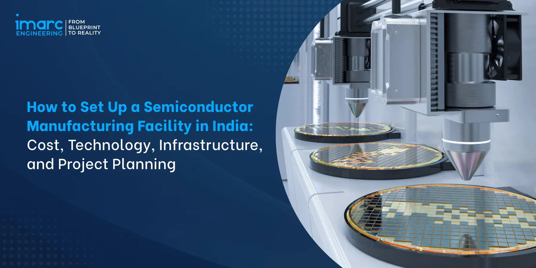
How to Set Up a Semiconductor Manufacturing Facility in India: Cost, Technology, Infrastructure, and Project Planning
Introduction
For investors and manufacturers evaluating India's semiconductor value chain in 2026, planning a semiconductor manufacturing facility in India demands disciplined evaluation across facility model selection, technology choice, capital planning, site conditions, utilities, cleanroom infrastructure, regulatory approvals, and project execution capability.
Semiconductor manufacturing spans wafer fabrication, compound semiconductors, and OSAT or ATMP operations, each with fundamentally different technology, capital, and infrastructure requirements.
Scope of this Guide
This guide answers the sponsor's project question directly. How can investors plan and establish a technically viable, commercially sustainable facility by evaluating technology, infrastructure, investment, site conditions, and execution needs? It walks through the market opportunity, setup roadmap, facility model and technology selection, capacity and site decisions, equipment and semiconductor cleanroom infrastructure, utilities design, regulatory approvals, and the practices distinguishing well-planned semiconductor plant setup in India from ad-hoc project entries.
Table of Contents
- Introduction
- Why Semiconductor Manufacturing Matters in India
- How to Set Up a Semiconductor Manufacturing Facility in India
- Semiconductor Facility Model and Technology Selection in India
- Capacity Planning and Site Selection for Semiconductor Plants in India
- Semiconductor Manufacturing Equipment and Cleanroom Infrastructure in India
- Utilities and Infrastructure Requirements for Semiconductor Fabs in India
- Regulatory Approvals and Compliance for Semiconductor Manufacturing in India
- Common Mistakes and Best Practices
- Conclusion
1. Why Semiconductor Manufacturing Matters in India
Four drivers make semiconductor manufacturing a strategic opportunity for Indian investors and technology partners in 2026.
1.1 India Semiconductor Mission and Policy Support
India Semiconductor Mission (ISM), established in December 2021 under the Ministry of Electronics and Information Technology (MeitY), launched the INR 76,000 crore Semicon India Programme covering silicon fabs, display fabs, compound semiconductors, ATMP or OSAT, and the Design Linked Incentive (DLI) scheme. ISM 2.0, approved by the Union Cabinet in July 2026, expanded the programme with additional financial outlay supporting further semiconductor manufacturing in India projects across facility categories. Central schemes provide 50 percent fiscal support on approved project cost for eligible categories.
Under ISM 1.0, the government approved 12 semiconductor manufacturing projects across six states with cumulative committed investment exceeding INR 1.64 lakh crore. Several of these projects have progressed from approval toward production. Micron's ATMP facility is in commercial production as of mid-2026, with additional approved units expected to come online through the remainder of the year.
The transition of approved projects into commercial production provides prospective investors with a growing base of domestic project experience across semiconductor packaging and manufacturing.
1.2 Demand-Side Growth
Domestic semiconductor demand grows rapidly across electronics, automotive, telecom, consumer devices, and industrial applications. India electronics production progressing supported by PLI schemes covering large-scale electronics manufacturing, IT hardware, and telecom equipment.
Automotive semiconductor demand grows with electric vehicle adoption and Advanced Driver Assistance Systems (ADAS) content. Data centre development in India and 5G infrastructure roll-out add commercial demand. Import substitution potential materially supports project economics for both domestic sales and export orientation.
1.3 State-Level Policy Alignment
State semiconductor policies supplement Central support. Gujarat Semiconductor Policy 2022-2027 provides additional capital subsidy on Central approved amounts. Uttar Pradesh Semiconductor Policy supports Jewar cluster development. Tamil Nadu Electronics Hardware Manufacturing Policy 2020 supports Chennai-Coimbatore cluster.
Karnataka Semiconductor Policy supports Bengaluru ecosystem. Odisha Semiconductor Manufacturing and Fabless Policy 2023 targets Bhubaneswar cluster. Assam State semiconductor engagement supports Jagiroad development. State layering on Central schemes significantly improves project economics for eligible investments.
1.4 Strategic Autonomy and Global Supply Chain Positioning
Global semiconductor supply chain diversification following geopolitical shifts creates opportunity for India as trusted manufacturing destination. Design talent depth across Bengaluru, Hyderabad, Pune, and NCR supports adjacent semiconductor manufacturing development.
Strategic partnerships with global technology companies and equipment suppliers support technology transfer. Domestic manufacturing supporting national strategic autonomy in critical electronics. India's positioning as neutral trusted manufacturing base supports both commercial and strategic project considerations.
2. How to Set Up a Semiconductor Manufacturing Facility in India
Understanding how to set up a semiconductor manufacturing facility in India helps sponsors sequence complex project decisions correctly. Setup integrates facility model selection, feasibility, ISM engagement, technology partnerships, engineering, construction, equipment installation, and qualification into coherent execution.
2.1 The Setup Roadmap
| Stage | Activities | Typical Duration |
|---|---|---|
| Facility Model and Market Assessment | Product strategy, technology roadmap, partner mapping | 3-6 months |
| Feasibility, DPR, and ISM Application | Techno-commercial evaluation, incentive application | 6-12 months |
| Technology and Equipment Partnerships | Licensor, cell fab partners, equipment vendors | 6-12 months (parallel) |
| Site Selection and Approvals | State engagement, environmental clearance, PESO | 9-18 months |
| Detailed Engineering | Cleanroom design, utilities, layout, tool hook-up | 9-15 months |
| Construction and Equipment Installation | Shell, cleanroom, tool move-in, hook-up | 18-30 months |
| Qualification and Ramp-Up | Tool qualification, yield ramp, customer qualification | 12-24 months |
2.2 Capex Opex and Financial Modelling for Semiconductor Projects in India
Capex, opex and financial modelling for semiconductor projects in India scale substantially with facility model and process technology. Semiconductor plant CAPEX for OSAT and ATMP facilities typically ranges from INR 1,500-15,000 crore.
Compound semiconductor fabs typically require INR 3,000-15,000 crore, while mature-node wafer fabs, such as those operating at 28-110 nanometres, may require INR 30,000-90,000 crore or more. Actual project CAPEX can vary substantially depending on production capacity, process technology, equipment configuration, cleanroom requirements, utility infrastructure, localisation, and the scope included in the investment estimate.
Central fiscal support under applicable semiconductor schemes, together with eligible state-level incentives, can materially influence project economics. The actual support available should be evaluated against the facility category, approved project cost, location, scheme conditions, and prevailing central and state policies.
2.3 Manufacturing Model Selection
Manufacturing model selection materially affects capital intensity, technology complexity, and time to market. OSAT and ATMP facilities offer lower capital intensity with faster market entry supporting India entry strategies. Compound semiconductor fabs targeting silicon carbide (SiC), gallium nitride (GaN), and gallium arsenide (GaAs) suit power electronics, RF, and optoelectronics applications with moderate capital.
Wafer fabrication plant for silicon front-end operations requires substantial capital and multi-year execution timelines but supports strategic long-term positioning. Model selection matched to promoter capability and market strategy supports sustainable positioning.
3. Semiconductor Facility Model and Technology Selection in India
Semiconductor facility model and technology selection in India determine the commercial foundation on which every downstream decision rests. Facility choice defines technology partnerships, capital intensity, workforce requirements, and market positioning.
3.1 Facility Categories Under ISM
| Facility Type | Scope |
|---|---|
| Silicon Wafer Fabrication | Front-end silicon wafer manufacturing (lithography, etch, deposition, implant) |
| Display Fab | LCD, OLED, flat panel display manufacturing |
| Compound Semiconductor Fab | GaN, SiC, GaAs wafer manufacturing for RF, power, optoelectronics |
| Silicon Photonics Fab | Integrated photonic circuits for data centre and communications |
| Sensors Fab | MEMS, imaging, biosensors manufacturing |
| ATMP or OSAT | Assembly, testing, marking, packaging of chips |
3.2 Process Node Selection for Wafer Fabs
Process-node selection should be driven by the intended product portfolio, customer requirements, technology access, equipment availability, yield targets, and project economics. Mature-node technologies can serve automotive, industrial, power-management, analogue, and connectivity applications, while more advanced nodes generally require substantially greater technology capability, equipment sophistication, and capital investment.
Advanced nodes at 7-14 nanometre serve high-performance computing but require substantially higher capital and technology complexity. Leading edge below 7 nanometre requires investment beyond typical India entry scale. India Semiconductor Mission approvals to date concentrate on mature and trailing edge nodes appropriate for domestic and export market segments.
3.3 Compound Semiconductor Technology Options
Compound semiconductor technology selection depends on target applications. Silicon Carbide (SiC) suits high-voltage power electronics for electric vehicles, renewable energy inverters, and industrial motor drives. Gallium Nitride (GaN) suits RF power amplifiers, fast charging, and 5G infrastructure. Gallium Arsenide (GaAs) suits RF and optoelectronic applications including laser diodes.
Indium Phosphide (InP) suits high-speed optical communications. Compound semiconductor fabs require moderate capital versus silicon fabs with specialised equipment and materials handling supporting attractive commercial positioning for niche applications.
3.4 OSAT and ATMP Technology Choices
OSAT and ATMP technology selection considers package types across wire bond, flip chip, wafer level packaging, System in Package (SiP), and 2.5D or 3D advanced packaging. Wire bond suits mature product packaging with lowest capital intensity. Flip chip and advanced packaging suit high-performance applications with higher capital requirements.
Wafer level packaging supports mobile and consumer electronics. Advanced packaging including 2.5D and 3D increasingly critical for AI accelerators and high-performance computing. Technology matched to target product mix supports commercial economics.
4. Capacity Planning and Site Selection for Semiconductor Plants in India
Capacity planning and site selection for semiconductor plants in India establish operational foundations that subsequent engineering decisions build upon. Site conditions particularly matter for semiconductor manufacturing given extreme sensitivity to vibration, air quality, and utility stability.
4.1 Capacity Metrics by Facility Type
| Facility | Capacity Metric |
|---|---|
| Silicon wafer fab | Wafer starts per month (WSPM), typically 10,000-100,000+ |
| Compound semiconductor fab | Wafer starts per month, typically 5,000-50,000 |
| OSAT or ATMP | Chip units per month or per year |
| Display fab | Substrate throughput, generation-based (Gen 8, Gen 10.5) |
4.2 Site Selection Criteria
- ISM cluster support across Gujarat (Dholera, Sanand), Assam (Jagiroad), Tamil Nadu, Karnataka, Odisha, and Uttar Pradesh
- State semiconductor policy providing additional capital subsidy
- Ultra-reliable power supply supporting 24x7 continuous operations
- Substantial water availability for ultra-pure water systems
- Seismic zone considerations for vibration-sensitive lithography equipment
- Air quality supporting cleanroom operations and reduced HVAC load
- Workforce access including engineers, technicians, and operators
- Airport and port connectivity for equipment imports and specialty gas supply
- Land availability with expansion potential
- Technology partner and equipment vendor accessibility
4.3 India Semiconductor Cluster Landscape
Semiconductor manufacturing site selection in India typically prioritises established or developing semiconductor clusters supporting ecosystem access. Dholera Special Investment Region and Sanand in Gujarat host wafer fab and ATMP operations. Jagiroad in Assam hosts OSAT operations. Bengaluru cluster in Karnataka supports design and adjacent manufacturing.
Chennai-Coimbatore corridor in Tamil Nadu supports electronics manufacturing ecosystem. Bhubaneswar cluster in Odisha targets compound semiconductor development. Jewar in Uttar Pradesh targets display and semiconductor operations. Cluster selection depends on facility model, state policy alignment, and infrastructure fit.
Cluster evaluation should also consider access to semiconductor-grade chemicals, specialty gases, spare parts, equipment service support, packaging materials, logistics for high-value imported tools, and qualified maintenance vendors. For facilities dependent on imported equipment and process materials, supplier lead times, customs handling, inventory strategy, and business-continuity planning can materially influence both ramp-up and long-term operating reliability.
4.4 Site Physical Requirements
Site physical requirements for semiconductor facilities are typically more demanding than those for conventional manufacturing plants. Site assessment should consider geotechnical conditions, external vibration sources such as railways, highways, and nearby heavy industry, ambient air quality, flood and drainage risk, and ground stability for equipment foundations and utility infrastructure.
For vibration-sensitive processes such as lithography and precision metrology, site vibration characteristics and structural isolation requirements should be evaluated against the specifications of the selected process equipment. Seismic conditions should similarly be assessed as part of structural and equipment-specific engineering rather than using a single seismic-zone criterion for all semiconductor facilities.
Land requirements depend on the facility model, production capacity, cleanroom footprint, central utility plant, chemical and gas infrastructure, logistics areas, safety requirements, and future expansion plans. Structured site assessment during feasibility helps identify physical constraints before major capital commitments are made.
5. Semiconductor Manufacturing Equipment and Cleanroom Infrastructure in India
Semiconductor manufacturing equipment and cleanroom infrastructure in India represent the largest capex components after building shell. Equipment selection and cleanroom design during engineering stage determine facility capability, yield potential, and product portfolio.
5.1 Core Wafer Fab Equipment
- Photolithography scanners or steppers (ASML, Canon, Nikon depending on node)
- Dry etch systems (plasma, reactive ion etch)
- Wet etch and cleaning systems
- Chemical Vapour Deposition (CVD) systems including PECVD and LPCVD
- Atomic Layer Deposition (ALD) systems
- Physical Vapour Deposition (PVD) sputter systems
- Ion implantation systems (registered under AERB for radiation-emitting equipment)
- Chemical Mechanical Planarisation (CMP) systems
- Rapid Thermal Processing (RTP) and diffusion furnaces
- Metrology and inspection tools (CD-SEM, ellipsometers, defect inspection)
- Wafer handling and automation systems (OHT, stockers)
5.2 Assembly and Testing Equipment for OSAT
- Wafer probers for wafer-level testing
- Wafer dicing and grinding equipment
- Die bonders and flip chip bonders
- Wire bonders (gold, copper, aluminium)
- Molding and encapsulation systems
- Automated Test Equipment (ATE) for final testing
- Marking, lasering, and packaging systems
- Burn-in and reliability testing chambers
5.3 Cleanroom Design and Classification
Cleanroom design follows ISO 14644-1 international standard for airborne particulate contamination classification. Wafer fab critical areas typically require ISO Class 1 to Class 4 supporting sub-micron particulate control. Compound semiconductor fabs typically require ISO Class 4-6. OSAT and ATMP facilities typically require ISO Class 5-8 depending on assembly complexity.
Cleanroom infrastructure includes HEPA and ULPA filtration, laminar airflow, temperature control typically to plus-minus 0.1 degree Celsius, humidity control, vibration isolation, and Airborne Molecular Contamination (AMC) control. Cleanroom engineering represents specialised discipline requiring experienced design partners.
5.4 Automation and Fab Software
Fab automation infrastructure supports operational efficiency and product quality. Automated Material Handling System (AMHS) including Overhead Hoist Transport (OHT) and stockers moves wafers between tools. Manufacturing Execution System (MES) provides production monitoring, dispatching, and traceability. Advanced Process Control (APC) systems support real-time process optimisation.
Yield Management System (YMS) enables defect analysis and yield improvement. Statistical Process Control (SPC) integrated across tools. Semiconductor Equipment Communication Standard (SECS) and Generic Equipment Model (GEM) protocols enable equipment integration. Digital manufacturing infrastructure distinguishes competitive fabs from those relying on legacy systems.
6. Utilities and Infrastructure Requirements for Semiconductor Fabs in India
Utilities and infrastructure requirements for semiconductor fabs in India exceed conventional manufacturing standards in scale, purity, and reliability. Utility infrastructure often represents 20-30 percent of total project cost and directly impacts operational yield.
6.1 Ultra-Pure Water Systems
Ultra-Pure Water (UPW) systems produce water at the highest industrial purity levels for wafer rinse and process applications. UPW quality parameters include resistivity above 18.2 megohm-centimetre, total organic carbon below 1 part per billion, dissolved oxygen below 5 parts per billion, and microbial contamination essentially undetectable.
UPW plant capacity typically 500-5,000 cubic metres per day for wafer fabs, scaled accordingly for other facility types. Raw water source, pre-treatment, primary treatment, polishing, and distribution loop constitute a complete UPW system requiring specialist design and operation.
6.2 Specialty and Bulk Gas Systems
Semiconductor manufacturing consumes bulk gases including nitrogen, oxygen, hydrogen, argon, and helium plus specialty gases including silane, arsine, phosphine, boron trichloride, ammonia, and hydrogen chloride. Bulk gas plants often located on-site or supplied through pipeline from adjacent industrial gas facility. Specialty gas cylinder yards and Valve Manifold Boxes (VMB) distribute gases to tools.
Toxic gas monitoring, emergency isolation, scrubbing, and abatement systems support safety compliance. Petroleum and Explosives Safety Organisation (PESO) licensing under Gas Cylinders Rules 2016 and Static and Mobile Pressure Vessels (Unfired) Rules 2016 governs gas storage and distribution.
6.3 HVAC, Chilled Water, and Process Cooling
HVAC infrastructure supports cleanroom operations with precise temperature and humidity control. Temperature stability typically plus-minus 0.1 degree Celsius in critical lithography bays. Humidity control typically 40-45 percent relative humidity with plus-minus 1 percent stability. Massive air recirculation with HEPA and ULPA filtration.
Chilled water systems supporting HVAC and process cooling typically requiring 5,000-30,000 tons refrigeration for wafer fabs. Process Cooling Water (PCW) loops distributed to tools. Redundancy across all utility systems supporting 24x7 operations preventing yield-affecting excursions.
6.4 Power, Chemicals, and Waste Treatment
Electrical infrastructure typically 20-100 megawatts for wafer fabs, 5-25 megawatts for compound semiconductor fabs, and 2-15 megawatts for OSAT operations. Uninterruptible Power Supply (UPS) and diesel generator backup supporting continuous operations. Chemical distribution systems for hydrofluoric acid, sulfuric acid, hydrogen peroxide, isopropyl alcohol, and photoresist.
Chemical waste treatment for acidic, basic, and organic streams. Gas abatement for toxic exhaust. Wastewater treatment including specific removal of fluorides, heavy metals, and organics before discharge. Comprehensive utility management distinguishes reliable fabs from those experiencing frequent excursions.
7. Regulatory Approvals and Compliance for Semiconductor Manufacturing in India
Regulatory approvals and compliance for semiconductor manufacturing in India span central incentive schemes, environmental approvals, safety compliance, and chemical or radiation-specific frameworks. Approval planning during feasibility prevents project delays.
7.1 India Semiconductor Mission Application
India Semiconductor Mission (ISM) under MeitY administers Central incentive schemes including Silicon Fab, Display Fab, Compound Semiconductor, and OSAT or ATMP sub-schemes with up to 50 percent fiscal support on approved project cost. Application requires detailed project proposal covering technology, financial capability, market strategy, execution capability, and technology partnership arrangements. Empowered Committee reviews and approves proposals.
Semicon 2.0, approved in July 2026 with a INR 1,27,500 crore outlay, expands India's semiconductor strategy across chip design, equipment and materials, fabrication, ATMP/OSAT, R&D, and talent development. State semiconductor policies provide supplementary capital subsidy on approved projects.
7.2 Environmental and Safety Approvals
The approvals applicable to a semiconductor facility depend on its location, process technology, chemicals and gases used, equipment configuration, project scale, and applicable central and state regulations. The following represents an indicative regulatory framework rather than a universal approval checklist.
| Approval | Authority | Trigger |
|---|---|---|
| Environmental Clearance | MoEFCC or SEIAA per EIA 2006 | Category A or B project scale |
| Consent to Establish | State Pollution Control Board | Pre-construction |
| Consent to Operate | State Pollution Control Board | Pre-commissioning |
| Factory Licence | State Directorate of Factories | Under OSH Code 2020 |
| Fire and life-safety approvals | Competent state/local authority | Per NBC 2016 Part 4 |
| Hazardous Waste Authorisation | SPCB under HOWM Rules 2016 | Chemical waste generation |
| MSIHC Compliance | PESO or Chief Inspector of Factories | Hazardous chemicals per MSIHC Rules 1989 |
| PESO Licence | PESO under Gas Cylinders Rules 2016 | Compressed and toxic gases |
| AERB Registration | Atomic Energy Regulatory Board | Ion implanters and X-ray equipment |
7.3 Chemical and Gas Safety Frameworks
Semiconductor manufacturing involves extensive hazardous chemicals and toxic gases requiring specific regulatory compliance. Manufacture, Storage and Import of Hazardous Chemicals (MSIHC) Rules 1989 as amended govern hazardous chemical handling with on-site emergency planning, off-site emergency planning, safety reports, and mock drills. Chemical Accidents (Emergency Planning, Preparedness and Response) Rules 1996 govern accident response frameworks.
Hazardous and Other Wastes (Management and Transboundary Movement) Rules 2016 as amended govern waste chemical management. Gas Cylinders Rules 2016 and Static and Mobile Pressure Vessels (Unfired) Rules 2016 govern gas storage. Comprehensive chemical safety planning during feasibility supports both compliance and operational safety.
7.4 Radiation and Import Compliance
Ion implantation equipment and certain X-ray-based metrology or inspection systems may require applicable approvals, registration, or authorisation from the Atomic Energy Regulatory Board (AERB), depending on the equipment and radiation source involved.
Import requirements, customs treatment, and any available duty concessions should be evaluated against prevailing customs notifications, project approvals, equipment classification, and the applicable incentive framework. Directorate General of Foreign Trade (DGFT) requirements may also apply depending on the equipment, materials, and import or export activities involved.
Projects considering a Special Economic Zone (SEZ) location should evaluate the current customs, fiscal, regulatory, and operational provisions applicable to their specific business model rather than relying on general or legacy SEZ benefits. Compliance planning across radiation, customs, trade, and related regulatory frameworks during feasibility supports more predictable project execution.
8. Common Mistakes and Best Practices
8.1 Facility Model Selection Without Market Fit
Facility model selection without validated market fit produces commercial vulnerability regardless of technical execution.
Best practice: product and market strategy validation before facility model commitment; addressable market quantification with target customer engagement; technology roadmap alignment with market direction; competitive positioning assessment against global players; documented offtake or customer engagement supporting bankability; model selection matched to promoter capability and capital availability.
8.2 Underestimating Utility Infrastructure
Utility infrastructure representing 20-30 percent of project cost routinely underestimated during initial feasibility produces both capex overrun and operational reliability issues.
Best practice: utility engineering during initial feasibility with specialist input; UPW, gas, HVAC, and chemical systems sized for capacity plus expansion; redundancy across critical systems preventing yield-affecting excursions; utility operations planning including specialist workforce and vendor arrangements; disciplined utility governance supporting operational stability.
8.3 Weak Technology Partnership Strategy
Semiconductor manufacturing typically requires technology partnerships that projects underestimate during planning.
Best practice: technology licensor engagement during feasibility with structured negotiation; equipment vendor relationships across all major categories; workforce development partnerships with training and secondment arrangements; customer qualification engagement supporting demand ramp; ecosystem participation through industry associations. Strong technology partnerships materially reduce execution risk that go-it-alone strategies typically cannot manage.
8.4 Cleanroom and Vibration Under-Investment
Cleanroom and vibration control under-investment produces persistent yield issues throughout facility life.
Best practice: cleanroom design with specialist engineering supporting ISO 14644-1 target class; vibration isolation for lithography and metrology equipment with civil design integration; Airborne Molecular Contamination (AMC) control matched to process sensitivity; HVAC redundancy supporting stable temperature and humidity; specialist commissioning and validation supporting cleanroom performance. Under-investment savings during construction produce recurring yield costs across operational life.
8.5 Regulatory and Chemical Safety Under-Preparation
Chemical safety and regulatory compliance under-preparation produces both approval delays and operational safety risks.
Best practice: comprehensive regulatory mapping during feasibility including MSIHC, PESO, AERB, and environmental frameworks; safety engineering integrated with facility design rather than retrofit; specialist safety workforce and emergency response infrastructure; insurance underwriter engagement supporting risk assessment; ongoing compliance management across operational life. Disciplined regulatory preparation prevents costly delays and incidents.
Conclusion
Planning a semiconductor facility in India in 2026 involves ISM opportunity assessment, facility model selection, technology and capacity planning, site selection, cleanroom and ultra-pure utility design, regulatory approvals, and technology partnerships. Central and state incentives can significantly improve project economics for eligible projects.
Three closing reminders for semiconductor sponsors. First, validate the facility model before downstream planning. Fab, compound semiconductor, OSAT/ATMP, and display projects differ significantly in capital, technology, timelines, and markets. Second, engineer UPW, specialty gases, HVAC, and chemical systems from feasibility onward. Third, integrate regulatory and chemical-safety planning early to support compliant, reliable operations.
PLANNING YOUR SEMICONDUCTOR MANUFACTURING FACILITY?
IMARC Engineering's semiconductor manufacturing facility and project development advisory team supports investors, sponsors, and semiconductor industry leaders across market opportunity assessment covering wafer fab, compound semiconductor, silicon photonics, sensors, OSAT and ATMP, and display fab facility categories, feasibility studies and Detailed Project Report (DPR) preparation aligned with India Semiconductor Mission (ISM) and ISM 2.0 requirements, technology and process node selection matched to market strategy, site selection support, utilities engineering, safety engineering, regulatory approvals, capex and opex financial modelling, technology partnership advisory, and disciplined project governance for semiconductor manufacturing facility development across India.
→ Schedule a free semiconductor facility scoping consultation with an IMARC specialist
Frequently Asked Questions
Setup follows seven stages: facility model and market assessment, feasibility with ISM application, technology and equipment partnerships, site selection and approvals, detailed engineering, construction and equipment installation, and qualification and ramp-up. Total programmes extend 30-72 months depending on facility category and scope.
Facility types under India Semiconductor Mission include silicon wafer fabrication plant, display fabs, compound semiconductor fabs (SiC, GaN, GaAs), silicon photonics, sensors fabs, and OSAT or ATMP facilities for assembly, testing, marking, and packaging. Each category has distinct capital and infrastructure requirements.
Semiconductor plant CAPEX varies substantially by facility type. OSAT and ATMP facilities typically require INR 1,500-15,000 crore. Compound semiconductor fabs typically require INR 3,000-15,000 crore. Legacy silicon wafer fabs at 28-110 nanometre nodes typically require INR 30,000-90,000 crore or higher including utilities.
Semiconductor plant infrastructure includes ultra-pure water (UPW) systems, bulk and specialty gases including silane, arsine, and phosphine, chemicals distribution, HVAC with precise temperature and humidity control, cleanroom facilities per ISO 14644-1, chilled water, uninterruptible power supply, and comprehensive chemical and gas waste treatment.
Semiconductor manufacturing equipment includes photolithography scanners, dry and wet etch systems, deposition tools (CVD, PVD, ALD), ion implanters registered under AERB, chemical mechanical planarisation, thermal processing furnaces, metrology and inspection tools, plus wafer probers, wire bonders, molding, and test equipment for OSAT operations.
Location selection considers the presence of semiconductor and electronics ecosystems, applicable state incentives, power and water requirements, site vibration and geotechnical conditions, workforce availability, logistics connectivity, technology-partner access, supply-chain support, and future expansion potential.
Approvals include Environmental Clearance under EIA 2006, SPCB Consent to Establish and Consent to Operate, Factory Licence under OSH Code 2020, Fire NOC per NBC 2016 Part 4, PESO for gases, MSIHC Rules 1989 compliance, and AERB registration, wherever applicable, for radiation-emitting equipment.
Semiconductor project feasibility depends on validated facility model matched to market demand, technology and process node fit, ISM and state incentive alignment, site infrastructure supporting utility-intensive operations, cleanroom and vibration control adequacy, workforce and technology partner availability, and project execution discipline across long timelines.
Recent Post

Trusted by Industry Leaders
We partner with global enterprises and ambitious businesses across sectors to deliver operational excellence, strategic insights, and sustainable growth through integrated solutions.












Success in Their Words
Real feedback from clients across industries. Discover how our solutions delivered measurable impact and operational excellence.

I wanted to express my sincere appreciation for your efforts in handling this matter. Your dedication and commitment have been truly commendable, and it is evident that you have put in tremendous hard work and expertise into resolving the issues at hand. We are greatly interested in continuing our collaboration with you in the future, as your professionalism and reliability have made you a trusted partner. Thank you once again for your invaluable contribution. We look forward to strengthening our partnership ahead.

It has been a pleasure working with the IMARC team. The insights provided were structured, clear, and highly valuable, helping us strengthen both our technical and financial planning with confidence. We deeply appreciate the team’s professionalism, responsiveness, and attention to detail throughout the engagement. Every requirement was well understood and effectively incorporated, resulting in a comprehensive and actionable output. Overall, our experience has been excellent, and I would gladly recommend IMARC to organizations seeking a reliable research partner.

Your service is truly exceptional. Working with the IMARC team has been a seamless and professional experience. The clarity of communication, responsiveness to queries, and consistent support at every stage made the entire engagement highly efficient. The insights shared were well-structured, practical, and perfectly aligned with our requirements, helping us make informed decisions with confidence. Overall, the dedication and professionalism demonstrated by your team stand out, and I would be glad to recommend IMARC as a reliable and trustworthy research partner.

IMARC did an outstanding job in preparing our study. They were punctual, precise, and consistently responsive throughout the entire process. The team delivered all the data we required in a clear, well-organized, and highly professional format. Their strong attention to detail, combined with their ability to meet every deadline without compromising quality, truly set them apart. Overall, their reliability and commitment made them an exceptional partner for our project, and we would gladly work with them again in the future.

IMARC made the whole process incredibly easy from start to finish. Everyone I interacted with via email was polite, professional, and straightforward to deal with, always keeping their promises regarding delivery timelines and remaining consistently solutions-focused. From my very first contact, I appreciated the professionalism and support shown by the entire IMARC team. I highly recommend IMARC to anyone seeking timely, affordable, and reliable information or advice. My experience with IMARC was excellent, and I truly cannot fault any aspect of it.

I’d like to express my sincere gratitude for the excellent work you accomplished with the study. Your ability to quickly understand our requirements and deliver high-quality results under tight timelines truly reflects your expertise, exceptional work ethic, and unwavering commitment to your customer’s success. The professionalism and responsiveness you demonstrated throughout the process made a significant difference. Our entire team and company are incredibly thankful for your dedication, reliability, and support. Once again, thank you for your outstanding contribution.