Manufacturing
September 29 2026
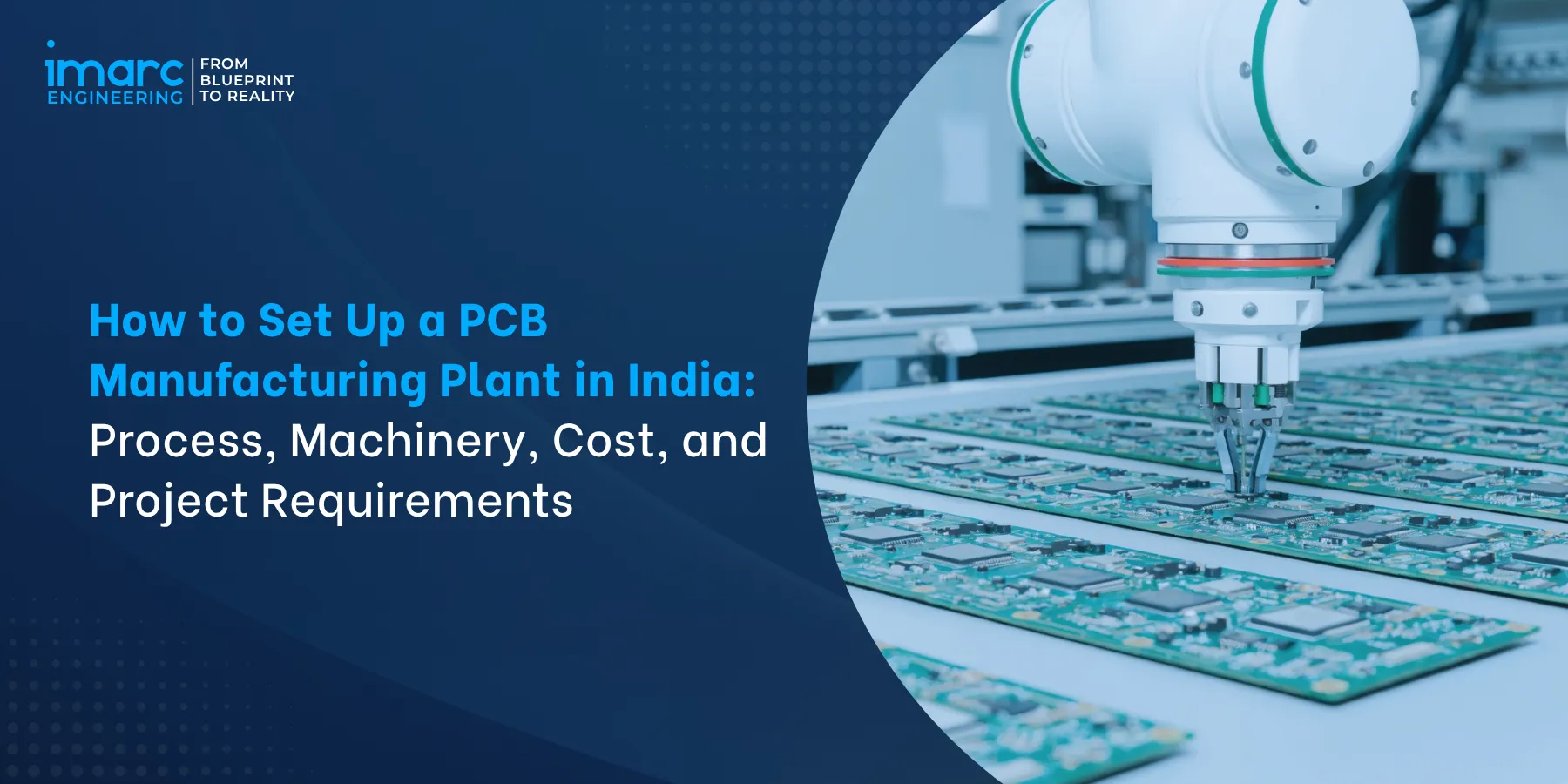
How to Set Up a PCB Manufacturing Plant in India: Process, Machinery, Cost, and Project Requirements
Introduction
For investors, electronics manufacturers, and project sponsors planning a PCB manufacturing plant in India in 2026, disciplined integration across PCB technology, production capacity, process design, machinery selection, cleanroom infrastructure, utilities, chemical management, wastewater treatment, and regulatory compliance determines commercial viability. India imports over 85 percent of PCB requirements today, and the Electronics Component Manufacturing Scheme (ECMS) with INR 22,919 crore outlay - covering multi-layer PCBs with additional 1 percent incentive on domestic laminate - has created a decisive policy window.
Scope of this Guide
This guide answers the sponsor's core question directly. How should investors plan a PCB production plant covering technology choice, product mix, machinery, chemicals, cleanroom, utilities, environmental compliance, CAPEX/OPEX, and project execution? It walks through PCB type and capacity planning, raw material and chemical requirements, drilling/imaging/plating/etching, lamination and solder mask, surface finishing and testing, cleanroom and utility infrastructure, ETP with CPCB Schedule VI or ZLD, hazardous waste under 2016 Rules, SPCB CTE/CTO, and CAPEX drivers - anchored to explicit assumptions.
Table of Contents
- Introduction
- Why PCB Manufacturing Plant Investment Matters for India in 2026
- What a PCB Manufacturing Plant is and Why It Matters in India
- PCB Type Layer Count and Capacity Planning for PCB Manufacturing Plants in India
- Raw Materials and Chemicals for PCB Manufacturing in India
- Drilling Imaging Plating and Etching for PCB Manufacturing in India
- Lamination Solder Mask Surface Finish and Testing for PCB Manufacturing Plants in India
- Machinery Cleanroom and Utilities for PCB Manufacturing Plants in India
- Wastewater Treatment Licences and Project Economics for PCB Manufacturing Plants in India
- Conclusion
1. Why PCB Manufacturing Plant Investment Matters for India in 2026
Four drivers make disciplined PCB manufacturing plant investment strategically important for manufacturers and project sponsors in 2026.
1.1 Import Dependence and Localization Push
India's electronics manufacturing sector has grown nearly six-fold over the past decade, but PCB manufacturing in India remains vastly under-served. Domestic capacity covers less than 15 percent of national demand across mobile phones, automotive electronics, industrial controls, telecom, consumer electronics, and defence. The remainder is imported primarily from China, Taiwan, South Korea, and Vietnam. This exposes downstream electronics manufacturers to supply-chain risk, currency fluctuation, and geopolitical uncertainty - making domestic PCB capacity a strategic priority.
1.2 Policy Framework Maturation
India's PCB manufacturing policy framework has strengthened meaningfully. The Electronics Component Manufacturing Scheme (ECMS) covers multi-layer PCBs as a target segment. It provides both turnover-linked and capital expenditure support, with an additional 1 percent incentive on domestic sourcing/manufacturing of laminate for multi-layer PCBs - directly encouraging vertical integration.
Incentive period runs FY 2026-27 to FY 2031-32. It complements the existing PLI for Large Scale Electronics Manufacturing (4-6 percent on incremental sales), SPECS (25 percent capital expenditure incentive), and Modified Electronics Manufacturing Clusters (EMC 2.0) providing plug-and-play infrastructure.
1.3 Investment Ecosystem
Multiple factors support PCB plant investment in India. Growing demand base from mobile manufacturing (India is the second-largest mobile phone producer globally), automotive electronics, and industrial applications. ECMS financial incentives reduce CAPEX/OPEX gaps versus imports. EMC 2.0 cluster infrastructure at YEIDA and other locations.
Recent ECMS approvals include Vital Electronics (multi-layer PCB in Maharashtra) and Ascent-K Circuits (advanced PCB at YEIDA). Indian Printed Circuit Association (IPCA) coordinates policy engagement. State-level industrial policies in Tamil Nadu, Maharashtra, Karnataka, Uttar Pradesh, and Andhra Pradesh offer land, power, and additional incentives.
1.4 Cost of Poor Planning
Poor project planning carries meaningful cost. Undersized cleanroom infrastructure limits throughput of high-value HDI or advanced multilayer products. Inadequate wastewater treatment triggers SPCB shutdown orders - PCB effluents contain heavy metals (copper, nickel, lead), acids, alkalis, and complex chelates requiring segregated treatment streams. Poor chemical management creates safety incidents and PESO non-compliance.
Insufficient IPC quality systems generate customer rejections. Late environmental clearance delays commissioning by 6-18 months (indicative). Integrated discipline across technology, capacity, machinery, utilities, chemicals, wastewater, and regulatory approvals reduces delivery risk and preserves ECMS eligibility.
2. What a PCB Manufacturing Plant is and Why It Matters in India
Understanding what a PCB manufacturing plant is and why it matters in India establishes the technology and infrastructure baseline for informed investment decisions.
2.1 Plant Definition
A printed circuit board manufacturing plant transforms copper-clad laminate into finished PCBs through sequential wet and dry processes: laminate cutting, drilling, electroless copper, imaging, electrolytic plating, etching, multilayer lamination, solder mask, surface finishing (HASL/ENIG/OSP), routing, electrical testing, and inspection. PCB plants are chemical-intensive facilities requiring segregated wet chemistry areas, cleanroom conditions for imaging, and specialized wastewater treatment for heavy-metal-bearing effluents. Product complexity ranges from single-sided consumer PCBs to advanced HDI and flex-rigid boards.
2.2 Plant Sections
| Section | Function | Key Equipment |
|---|---|---|
| Laminate prep | Cutting, scoring, cleaning | Cutters, brushing machines |
| Drilling | Through-holes, microvias | CNC drilling, laser drilling |
| Wet chemistry | Electroless copper, plating | Plating lines, tanks |
| Imaging | Photoresist, exposure, develop | Dry film, LDI/UV exposure |
| Etching | Copper pattern definition | Etching lines, strippers |
| Multilayer | Lay-up, press, oxide | Lamination press, oxide line |
| Solder mask | Protection layer application | LPI print, expose, develop |
| Surface finish | HASL, ENIG, OSP, immersion | HASL machine, ENIG line |
| Testing | Electrical, AOI, visual | Flying probe, AOI, microscopy |
| Utilities/ETP | DI water, HVAC, wastewater | DI plant, chillers, ETP |
2.3 Plant Scale Determinants (Figures are Indicative in Nature)
Plant scale depends on product complexity, capacity target, and business model. Single/double-sided consumer PCB plants target INR 30-100 crore CAPEX. Standard multilayer plants (4-8 layer for automotive, industrial, telecom) require INR 100-500 crore for medium capacity. Advanced multilayer plants (10+ layer, HDI, flex-rigid) for mobile, telecom infrastructure, and defence applications require INR 500-2,000 crore or more.
Cleanroom class, wet chemistry line count, imaging technology (UV versus LDI), and testing capability drive CAPEX intensity. Capacity is measured in square metres of PCB per month (SqM/month), with medium plants producing 20,000-60,000 SqM/month and large plants above 100,000 SqM/month.
3. PCB Type Layer Count and Capacity Planning for PCB Manufacturing Plants in India
Understanding PCB type layer count and capacity planning for PCB manufacturing plants in India is the foundational decision that cascades through machinery, cleanroom, and CAPEX.
3.1 PCB Types
PCB technology spans several categories. Single-layer PCB has copper on one side of laminate - lowest cost, used in consumer/LED applications. Double-sided PCB has copper on both sides connected through plated through-holes - workhorse for consumer/industrial. Multilayer PCB (4-40+ layers) uses stacked copper and dielectric - required for complex electronics, automotive, telecom. HDI PCB uses microvias (laser-drilled below 150 microns) and fine-line traces - critical for mobile devices. Flexible PCB uses polyimide substrates for bendable applications. Flex-rigid combines rigid and flex sections. Each drives distinct machinery, chemistry, and yield requirements.
3.2 Capacity Planning (Figures are indicative in Nature, may vary)
Capacity planning for PCB plants combines area throughput (SqM/month or panels/month) with product mix. Small-medium plants: 5,000-30,000 SqM/month typically for single/double-sided products, INR 30-100 crore. Medium plants: 30,000-80,000 SqM/month for standard multilayer, INR 100-500 crore. Large plants: 80,000-200,000 SqM/month for advanced multilayer/HDI, INR 500-2,000+ crore. Panel size (18"×24" or 21"×24") and layer mix affect effective throughput. Yield planning directly affects saleable capacity.
3.3 Product Mix Decisions
Product mix shapes the entire PCB plant design. Consumer electronics single/double-sided products fit small-medium plants with modest cleanroom and HASL surface finish. Automotive electronics require IATF 16949 quality systems, 4–8-layer PCBs, and thermal cycling qualification. Telecom infrastructure needs 10-20 layer high-frequency PCBs with controlled impedance. Mobile devices need HDI with 2-4 mil traces, microvia stacks, and ENIG or immersion silver finish. Defence applications require IPC Class 3 qualification and specialized processes. Multi-product plants require flexible line configuration.
3.4 Location and Cluster Selection
PCB plant location considers electronics ecosystem proximity (customer clusters in Tamil Nadu, Karnataka, Maharashtra, Uttar Pradesh, Andhra Pradesh, and Telangana), power and water reliability, EMC 2.0 cluster access, ETP infrastructure, skilled workforce, transport connectivity, and state incentive schemes. YEIDA, Tamil Nadu's Sriperumbudur-Oragadam belt, Karnataka's Bengaluru corridor, and Maharashtra's Navi Mumbai/Aurangabad zones host substantial electronics manufacturing. Greenfield PCB manufacturing plant projects also evaluate SPCB category classification early - PCB manufacturing typically falls in the Red category.
4. Raw Materials and Chemicals for PCB Manufacturing in India
Understanding raw materials and chemicals for PCB manufacturing in India covers the substrate, copper, and complex chemistry that transform bare laminate into finished boards.
4.1 Base Materials
Base materials center on copper-clad laminate (CCL). FR-4 (flame-retardant fiberglass-reinforced epoxy) dominates for standard PCBs across consumer and industrial applications, per IPC-4101 base material specification. CEM-1 serves lower-cost single-sided consumer applications. Polyimide substrates enable flex circuits. High-Tg FR-4 supports thermal cycling. Halogen-free variants meet environmental regulations. Prepreg (partially cured resin-impregnated glass fabric) provides bonding between copper layers during multilayer lamination. Copper foil thickness ranges from 12 microns for HDI to 105 microns for power PCBs, with 35 microns standard. Domestic laminate manufacturing (encouraged by ECMS +1 percent incentive) improves project economics.
4.2 Process Chemistry
PCB wet processing uses many chemistry streams. Cleaning: alkaline degreasers and acid preclean. Electroless copper: palladium activation, then formaldehyde-reduced bath depositing 0.3-1 micron copper on hole walls. Electrolytic plating: acid copper sulphate baths (25-35 microns hole wall copper for standard boards). Tin plating: methanesulphonic acid-based tin as etch resist. Etching: cupric chloride (acid) or ammoniacal alkaline etchants. Resist stripping: sodium hydroxide-based. Oxide/brown oxide for multilayer bonding. Solder mask: liquid photoimageable (LPI) inks. Surface finish: HASL flux, ENIG (nickel + gold), OSP, or immersion silver.
4.3 Consumables
Consumables for PCB production line operation include drill bits (carbide, 0.2-6.5 mm, life 2,000-10,000 hits), backup and entry boards, dry film photoresist rolls (25-50 micron), phototools or LDI systems, developer chemistry, laminate press cushions and release films, ENIG replenishment (nickel/gold salts), and specialized dielectrics for HDI stackups. Consumable cost is 15-25 percent of manufacturing cost.
4.4 Chemical Storage and Safety
Chemical storage requires dedicated areas with segregation by compatibility (acids, alkalis, oxidizers, flammables kept apart), secondary containment, ventilation, spill response, and MSDS accessibility. Bulk chemicals (sulphuric acid, hydrochloric acid, sodium hydroxide, ammonia) require corrosion-resistant tank farms with level monitoring and leak detection. Cyanide-bearing chemistry (if used) requires strict segregation from acid streams to prevent hydrogen cyanide generation. PESO approval applies where chemical storage crosses threshold quantities. Emergency shower/eyewash stations, fire suppression, and PPE are baseline safety infrastructure.
5. Drilling Imaging Plating and Etching for PCB Manufacturing in India
Understanding drilling imaging plating and etching for PCB manufacturing in India covers the core process technologies that define board precision and yield.
5.1 Drilling
Drilling creates through-holes and vias. CNC drilling uses multi-spindle machines (2-6 spindles per station) with carbide drills, typical range 0.2-6.5 mm, at 60,000-300,000 rpm depending on hole size. Drill quality directly affects plating and reliability - poor drilling causes hole wall roughness, smear, and delamination. Multi-panel stacks (1-3 panels for standard, single for HDI) balance throughput and precision. Laser drilling (CO2 or UV laser) creates microvias below 150 microns - essential for HDI applications. Post-drill deburring removes burrs, and hole cleaning (desmear via plasma or permanganate) removes drilling residue before electroless copper. Registration accuracy (typically ±25-50 microns) is critical for multilayer alignment.
5.2 Electroless Copper and Imaging
After drilling, electroless copper deposition coats hole walls with 0.3-1 micron copper - the seed for electrolytic plating. Panels then move to imaging. Dry film photoresist (25-50 micron) is laminated, exposed through phototool (conventional UV) or laser direct imaging (LDI), then developed. LDI dominates for HDI and fine-line applications (below 3 mil trace/space) - improves accuracy and turnaround. Imaging cleanroom class (Class 10,000-100,000, tighter for HDI) protects against defects. Registration accuracy drives multilayer yield.
5.3 Copper Plating
Electrolytic copper plating builds copper thickness on hole walls and exposed pad areas. Panel plating deposits copper across the panel before pattern definition; pattern plating deposits copper only in imaged areas plus tin as etch resist. Modern pulse and reverse-pulse (PPR) plating improve throwing power - uniform deposition in high-aspect-ratio holes (10:1 standard, up to 15:1 advanced). Target hole wall thickness is 25-35 microns for standard multilayer, up to 50 microns for backplane applications. Plating bath control (copper concentration, additives, temperature, current density) determines quality and yield.
5.4 Etching and Stripping
Etching removes unwanted copper to define the circuit pattern. Two chemistries dominate: acidic cupric chloride (regenerable, dominant for outer layers of double-sided/multilayer) and alkaline ammoniacal etchant (for inner layers of multilayer). Spray etchers with multiple chambers followed by rinse determine line width control. Undercut and side-wall profile affect fine-line yield. Tin resist is stripped chemically for pattern-plated products. Automated optical inspection (AOI) after etching detects opens, shorts, and line width deviations - a critical checkpoint.
6. Lamination Solder Mask Surface Finish and Testing for PCB Manufacturing Plants in India
Understanding lamination solder mask surface finish and testing for PCB manufacturing plants in India covers the finishing and quality steps that determine board reliability.
6.1 Multilayer Lamination
For multilayer PCB manufacturing India operations, inner-layer imaged and etched cores undergo oxide or brown-oxide treatment (micro-roughness for prepreg bonding), then are stacked with prepreg sheets and copper foil in the desired sequence. The stack enters a lamination press - vacuum press with heated platens at 175-200°C and 250-500 psi for 60-120 minutes. Modern presses use closed-loop temperature and pressure control. After lamination, panels are drilled for through connections and follow the drilling-plating-imaging-etching sequence for outer layers. Sequential lamination enables HDI stackups with buried and blind vias.
6.2 Solder Mask and Legend
Solder mask provides electrical insulation and solder confinement during assembly. Liquid Photoimageable (LPI) mask dominates - applied by screen print or spray coat, pre-cured, exposed through phototool or LDI, developed, and thermally cured. Standard colors include green, red, blue, yellow, black, and white; green remains most common for cost/quality reasons. Solder mask must meet IPC-SM-840 requirements. Legend printing (silkscreen or inkjet) adds component identifiers, polarity marks, and part numbers. Legend accuracy is important for downstream assembly ease and traceability.
6.3 Surface Finish
Surface finish protects exposed copper from oxidation and provides solderability. HASL (Hot Air Solder Levelling) dips panels in molten solder then removes excess with hot air knives - lowest cost, ubiquitous for standard products. Lead-free HASL uses SAC alloys. ENIG (per IPC-4552) deposits 3-6 microns nickel then 0.05-0.10 microns gold - flat surface suited for HDI, BGA, and fine-pitch applications. OSP applies organic azole compound - low cost, limited shelf life. Immersion silver (IPC-4553) and immersion tin serve specific applications. Choice depends on assembly technology, shelf-life, cost, and qualification.
6.4 Testing and Inspection
Every finished PCB undergoes electrical testing for continuity and isolation. Flying probe testers (2-8 probes) suit prototyping and low-medium volume without fixture cost. Bed-of-nails testers with dedicated fixtures suit high-volume standard products. Automated optical inspection (AOI) is applied after imaging, etching, and solder mask - detecting opens, shorts, line width deviation, and mask registration errors. Cross-section analysis per IPC-TM-650 validates hole wall copper thickness and multilayer registration. Ionic contamination and thermal shock testing validate reliability. Final visual inspection follows IPC-A-600.
7. Machinery Cleanroom and Utilities for PCB Manufacturing Plants in India
Understanding machinery cleanroom and utilities for PCB manufacturing plants in India covers the infrastructure that determines throughput, quality, and OPEX.
7.1 Key Machinery
| Category | Equipment | Illustrative Scale |
|---|---|---|
| Preparation | Cutting, scoring, brushing | 300-1,500 panels/hour |
| Drilling | CNC drills, laser drills | 3-6 spindles per station |
| Wet chemistry | Plating lines, etchers | Multi-tank horizontal/vertical |
| Imaging | Dry film, LDI/UV exposure | 50-300 panels/hour |
| Lamination | Vacuum press, oxide line | 8-16 opening presses |
| Finishing | HASL, ENIG, LPI mask | Line-specific throughput |
| Testing | Flying probe, AOI, e-test | Product-specific cycle |
| Utilities | DI plant, HVAC, chillers | 2-15 MW total plant |
7.2 Cleanroom Infrastructure
Cleanroom classification is critical for PCB yield. Standard multilayer imaging requires Class 10,000-100,000 (ISO 7-8). HDI and fine-line (below 3 mil) operations need Class 1,000-10,000 (ISO 6-7). Design considers HEPA-filtered air supply, positive pressure differentials, gowning protocols, controlled temperature (20-24°C) and humidity (45-55 percent RH), photoresist zones under yellow lighting, and material transfer through air locks. HVAC alone can be 15-25 percent of plant electrical load and directly affects yield.
7.3 Process Utilities
PCB plant utilities are substantial. Total electrical connected load 2-15 MW for medium plants, with UPS backup for critical equipment (drilling, plating rectifiers, AOI). Deionized water (1-3 microSiemens/cm) is essential for rinse - typical consumption 5-15 kL/day for medium plants, via reverse osmosis and mixed-bed polishing. HVAC covers cleanroom and general facility. Compressed air (oil-free, instrument-grade) supplies drilling, cleaning, and pneumatics. Chilled water at 7-12°C for process cooling. Exhaust scrubbing captures acid fumes, ammonia, and volatile emissions from wet chemistry areas - critical for worker safety and Air Act 1981 compliance. Backup DG sizing typically 60-80 percent of connected load.
7.4 Plant Layout and Material Handling
PCB plant layout separates wet chemistry areas (acid-resistant flooring, drainage to ETP, corrosion-resistant construction), imaging cleanroom, dry areas (drilling, mechanical operations), and support facilities. Material flow moves panels sequentially with minimal cross-contamination risk. Automated material handling (conveyors, panel racks) reduces damage. Cleanroom access follows strict gowning protocols. Chemical storage is separated from production. Utility corridors provide services without disrupting processes. Land requirement typically 2-10 hectares for medium plants. Layout is difficult and expensive to change post-construction.
8. Wastewater Treatment Licences and Project Economics for PCB Manufacturing Plants in India
Understanding licences environmental approvals and project economics for PCB manufacturing plants in India completes the framework for informed investment decisions.
8.1 Wastewater Treatment
PCB wastewater is chemically complex and requires specialized effluent treatment plant (ETP) design. Segregated collection separates streams by chemistry: acid streams (spent etchant, acid rinse), alkaline streams (developer, resist stripper), chelated streams (electroless copper - requires chelate breaking), and any cyanide streams. Treatment sequence: chelate breaking (oxidation, typically hydrogen peroxide), pH neutralization, heavy metal precipitation (copper, nickel, lead), coagulation-flocculation, sedimentation, sand/carbon filtration, and biological treatment where organic load requires it.
Treated effluent must meet CPCB Schedule VI limits. Water-stressed locations may require Zero Liquid Discharge (ZLD) via RO and multi-effect evaporation. OCEMS with real-time data to CPCB is standard for Red category units.
8.2 Hazardous Waste Management
Hazardous waste from PCB operations includes ETP sludge (copper-, nickel-, lead-bearing precipitates), spent plating solutions, spent etchants, chemical containers, and process residues. Management follows Hazardous and Other Wastes (Management and Transboundary Movement) Rules 2016. Requirements: hazardous waste authorization from SPCB, waste inventory maintenance, storage with secondary containment, transportation via authorized transporters, and disposal at SPCB-authorized TSDF. Copper recovery from spent etchants and sludge (through authorized recyclers) offers cost recovery and reduced disposal burden. E-Waste Rules 2022 apply to any electronic waste generated internally.
8.3 Regulatory Framework
PCB plants navigate multiple regulatory approvals. SPCB Consent to Establish (CTE) before construction and Consent to Operate (CTO) before production under Water Act 1974 and Air Act 1981. Hazardous waste authorization under 2016 Rules. Environmental Clearance under EIA Notification 2006 where capacity or investment thresholds are crossed.
Factory licence under OSH Code 2020. Fire NOC per NBC 2016. PESO approval for chemical storage above threshold quantities under MSIHC Rules 1989. E-Waste Rules 2022. State industrial approvals including SIA/EM-II. ECMS-specific approvals from MeitY where the scheme is availed.
8.4 Project Economics
| Configuration | Scale Assumption | Investment (INR) (Indicative, may vary) |
|---|---|---|
| Single/double-sided | Small-medium capacity | 30-100 crore |
| Standard multilayer (4-8L) | Medium capacity | 100-500 crore |
| Advanced multilayer/HDI | Medium-large capacity | 500-2,000 crore |
| Flex-rigid / mega HDI | Large capacity | 2,000+ crore |
8.5 CAPEX and OPEX Composition (Illustrative in Nature, may vary)
CAPEX composition for PCB plants: wet chemistry lines 20-30 percent; drilling 10-15 percent; imaging 8-12 percent; lamination press 5-10 percent; testing/AOI 8-12 percent; cleanroom/HVAC 10-15 percent; ETP and utilities 10-15 percent; civil 8-12 percent; engineering/commissioning 5-8 percent. OPEX drivers: raw materials 30-40 percent, chemicals 15-25 percent, electricity 10-15 percent, labour 8-15 percent, consumables 5-10 percent, waste disposal 3-5 percent. Yield loss is a major OPEX driver. Commissioning typically 12-18 months for standard multilayer; 18-24 months for advanced HDI/flex rigid.
Conclusion
Setting up a PCB manufacturing plant in India requires technology and capacity planning, base material sourcing, process design, utilities, ETP and waste management, regulatory compliance, and ECMS planning. Key processes include drilling, imaging, plating, etching, lamination, solder masking, surface finishing, electrical testing, and AOI, with infrastructure and commissioning requirements varying by product complexity.
Three priorities are critical. First, chemistry management and wastewater treatment must be planned from the outset. Second, cleanroom requirements, process control, and yield directly affect product quality and profitability. Third, ECMS eligibility and project structuring should be assessed early to align technology, investment, and incentive requirements.
PURSUING A PCB MANUFACTURING PLANT IN INDIA?
IMARC Engineering supports investors, electronics manufacturers, and project sponsors with PCB technology and capacity planning, site selection, raw material strategy, process design, utilities, ETP and waste management, regulatory compliance, ECMS structuring, and capital investment planning. The advisory covers conventional, multilayer, HDI, flex, and rigid-flex PCBs, including drilling, imaging, plating, etching, lamination, solder masking, surface finishing, testing, and quality control, with project-specific infrastructure and commissioning planning.
→ Schedule a free PCB manufacturing plant scoping consultation with an IMARC specialist
Frequently Asked Questions
PCB manufacturing plant in India setup requires product mix definition (single/double/multilayer), capacity planning, process design (drilling/imaging/plating/etching/lamination/soldermask/testing), specialized machinery, cleanroom infrastructure, utilities, environmental clearance, SPCB CTE/CTO, hazardous waste authorization under 2016 Rules, ETP with ZLD where mandated, quality systems, and staged commissioning over 12-24 months typically.
The PCB manufacturing process starts with copper-clad laminate preparation, drilling (CNC/laser), electroless copper deposition on hole walls, imaging (photoresist), electrolytic copper plating, etching to define circuit patterns, lamination for multilayer boards, solder mask application, surface finish (HASL/ENIG/OSP), routing, electrical testing, and automated optical inspection (AOI).
PCB manufacturing machinery includes laminate cutting/scoring, CNC drilling and laser drilling machines, electroless copper plating lines, imaging (LDI or photoresist), electroplating tanks, etching lines, oxide/brown oxide treatment, lamination press for multilayer boards, solder mask printing, surface finish lines (HASL/ENIG), routers, electrical testers, and AOI systems.
PCB raw materials include copper-clad laminate (FR-4/CEM-1/polyimide), prepreg, copper foil, and drill bits. Chemicals include electroless copper solutions, electroplating baths (acid copper/tin), photoresist, developer, cupric chloride etchant, solder mask ink, ENIG chemistry (nickel/gold), HASL flux, and cleaning solvents - all requiring hazardous chemical handling protocols.
PCB manufacturing plant cost in India depends on layer capability, capacity, and technology. Illustrative brackets: single/double-sided plants (small-medium) INR 30-100 crore; standard multilayer (4-8 layer) INR 100-500 crore; advanced HDI or flex-rigid facilities INR 500-2,000+ crore. ECMS provides 25 percent CAPEX incentive for eligible projects.
Higher layer count multilayer PCBs require lamination presses, sequential build capability, and precision drilling; HDI/microvia requires laser drilling; flex boards need polyimide handling. Higher capacity requires larger plating lines, imaging throughput, and testing capacity. Design mix drives cleanroom class, chemical consumption, and overall CAPEX intensity.
PCB plant utilities include reliable electricity (typically 2-15 MW for medium plants), deionized (DI) water for rinse operations, process water, HVAC with controlled cleanroom (Class 10,000-100,000), compressed air (oil-free), chilled water, hazardous chemical storage, exhaust scrubbing, effluent treatment plant (ETP), backup power, and support infrastructure.
PCB plant wastewater goes through segregated collection (acid/alkali/cyanide/chelated streams), primary neutralization, heavy metal precipitation (copper/nickel/lead removal), biological treatment, filtration, and final polishing. ETP achieves CPCB Schedule VI discharge limits or Zero Liquid Discharge (ZLD) where mandated. Hazardous sludge is disposed through authorized SPCB-registered TSDF facilities.
PCB quality control includes incoming material inspection, in-process microscopy for line width and hole geometry, plating thickness measurement, cross-section analysis, electrical testing (bare board), automated optical inspection (AOI) after imaging and finishing, thermal shock testing, ionic contamination testing, and final visual inspection per IPC-A-600 standards.
PCB plants require SPCB CTE/CTO under Water/Air Acts, hazardous waste authorization under 2016 Rules, Environmental Clearance if applicable, ETP compliance with CPCB Schedule VI limits or ZLD, OSH Code 2020 factory licence, PESO for chemical storage, Fire NOC per NBC 2016, and E-Waste Rules 2022.
Recent Post




Trusted by Industry Leaders
We partner with global enterprises and ambitious businesses across sectors to deliver operational excellence, strategic insights, and sustainable growth through integrated solutions.












Success in Their Words
Real feedback from clients across industries. Discover how our solutions delivered measurable impact and operational excellence.

I wanted to express my sincere appreciation for your efforts in handling this matter. Your dedication and commitment have been truly commendable, and it is evident that you have put in tremendous hard work and expertise into resolving the issues at hand. We are greatly interested in continuing our collaboration with you in the future, as your professionalism and reliability have made you a trusted partner. Thank you once again for your invaluable contribution. We look forward to strengthening our partnership ahead.

It has been a pleasure working with the IMARC team. The insights provided were structured, clear, and highly valuable, helping us strengthen both our technical and financial planning with confidence. We deeply appreciate the team’s professionalism, responsiveness, and attention to detail throughout the engagement. Every requirement was well understood and effectively incorporated, resulting in a comprehensive and actionable output. Overall, our experience has been excellent, and I would gladly recommend IMARC to organizations seeking a reliable research partner.

Your service is truly exceptional. Working with the IMARC team has been a seamless and professional experience. The clarity of communication, responsiveness to queries, and consistent support at every stage made the entire engagement highly efficient. The insights shared were well-structured, practical, and perfectly aligned with our requirements, helping us make informed decisions with confidence. Overall, the dedication and professionalism demonstrated by your team stand out, and I would be glad to recommend IMARC as a reliable and trustworthy research partner.

IMARC did an outstanding job in preparing our study. They were punctual, precise, and consistently responsive throughout the entire process. The team delivered all the data we required in a clear, well-organized, and highly professional format. Their strong attention to detail, combined with their ability to meet every deadline without compromising quality, truly set them apart. Overall, their reliability and commitment made them an exceptional partner for our project, and we would gladly work with them again in the future.

IMARC made the whole process incredibly easy from start to finish. Everyone I interacted with via email was polite, professional, and straightforward to deal with, always keeping their promises regarding delivery timelines and remaining consistently solutions-focused. From my very first contact, I appreciated the professionalism and support shown by the entire IMARC team. I highly recommend IMARC to anyone seeking timely, affordable, and reliable information or advice. My experience with IMARC was excellent, and I truly cannot fault any aspect of it.

I’d like to express my sincere gratitude for the excellent work you accomplished with the study. Your ability to quickly understand our requirements and deliver high-quality results under tight timelines truly reflects your expertise, exceptional work ethic, and unwavering commitment to your customer’s success. The professionalism and responsiveness you demonstrated throughout the process made a significant difference. Our entire team and company are incredibly thankful for your dedication, reliability, and support. Once again, thank you for your outstanding contribution.