India's Semiconductor Manufacturing Expansion Gains Momentum with 12 Approved Facilities
May 14, 2026
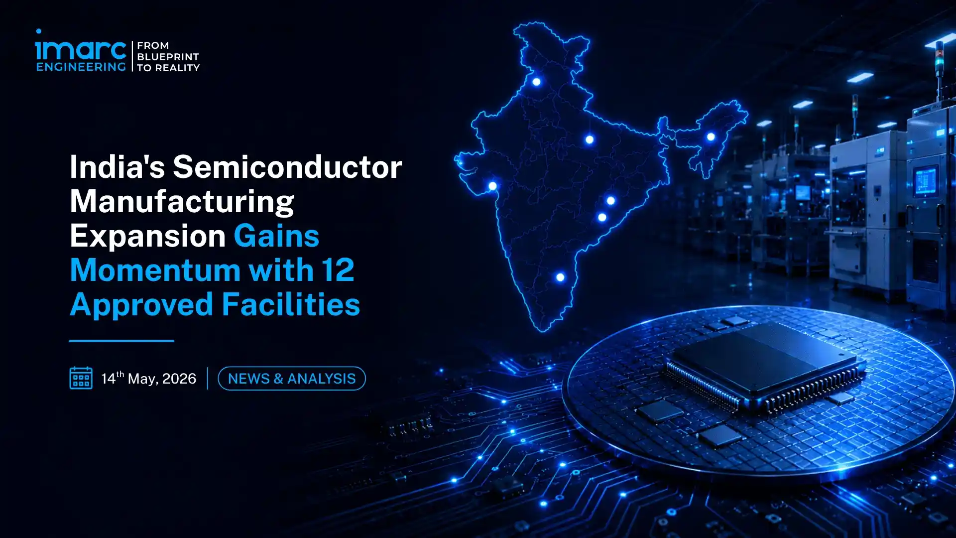
The expansion of semiconductor manufacturing in India crossed a significant threshold on May 5, 2026, when the Union Cabinet approved two additional semiconductor manufacturing projects under the India Semiconductor Mission (ISM), bringing the total count of approved facilities to 12 across six states, with cumulative investments of approximately Rs 1.64 lakh crore.
Three weeks earlier, on April 9, the government notified Special Economic Zone status for Tata Electronics' Dholera fab site, a 66-hectare facility with an on-site inland container depot. In line with this, on February 28, Prime Minister Modi inaugurated Micron Technology's assembly, test, marking, and packaging (ATMP) facility in Sanand, Gujarat, the first operational semiconductor facility of the current mission cycle. Taken together, these milestones mark the point at which India's semiconductor ambition has moved decisively from policy intent to physical infrastructure.
The current wave of India semiconductor expansion is being driven by a combination of government incentives, global supply chain diversification, and rising domestic demand for electronics and chip-enabled technologies.
Semiconductor Manufacturing in India: From 6 to 12 Approved Projects in 15 Months
The India semiconductor mission was established in December 2021 under a Rs 76,000 crore incentive framework, offering fiscal support of up to 50% of project cost for silicon fabs, compound semiconductor units, ATMP and OSAT facilities, and chip design projects. The pace of project approvals has accelerated sharply. The first six approvals covered the three anchor facilities, Tata Electronics Dholera fab, Tata Semiconductor Assembly and Test (TSAT) in Assam, and CG Power's OSAT unit in Sanand, alongside Micron's ATMP facility.
On August 12, 2025, four more projects were approved: SiCSem Private Limited's Silicon Carbide fab in Bhubaneswar, Odisha (India's first commercial SiC compound semiconductor fabrication facility, with Clas-SiC Wafer Fab Ltd. of the UK as technology partner); 3D Glass Solutions' advanced glass substrate and interposer packaging facility in Odisha; CDIL's high-power discrete semiconductor manufacturing expansion at Mohali, Punjab; and a fourth facility in Andhra Pradesh, collectively drawing Rs 4,600 crore and generating over 2,000 jobs.
The May 5, 2026 approvals added two more: Crystal Matrix Limited (CML), which will establish an integrated compound semiconductor fabrication and ATMP facility in Dholera for Mini/Micro-LED display modules and GaN foundry services including epitaxy on 6-inch wafers; and Suchi Semicon Private Limited (SSPL), which will set up an OSAT facility in Surat, Gujarat, with a production capacity of 1,033 million chips per annum serving power electronics, analog ICs, automotive, and industrial systems markets. The combined investment for the two May approvals is Rs 3,936 crore, with 2,230 skilled jobs projected.
The Union Budget 2026-27 allocated Rs 8,000 crore to the semiconductor mission, the largest single-year outlay since the programme launched, alongside the announcement of ISM 2.0, focused on semiconductor equipment and materials manufacturing, advanced design capability, and indigenous IP development.
Semiconductor Facilities in India: The Geography of the Buildout
Gujarat has emerged as the unambiguous semiconductor capital of India. Of the 12 approved projects, four are in Gujarat, three of them in Sanand alone. Sanand is establishing itself as India's first true ATMP hub: Micron's $2.75 billion ATMP facility (inaugurated February 28, 2026) will produce DRAM and NAND flash memory chips for mobile devices, data centres, and automotive applications. CG Power's G1 OSAT pilot line, inaugurated August 28, 2025, can handle 0.5 million chip units per day, with the G2 facility scaling to 14.5 million units per day and creating over 5,000 jobs.
Kaynes Semicon's OSAT unit in Sanand reached commercial production in March 2026, just 14 months after breaking ground, shipping India's first commercially produced 900 multi-chip modules to Alpha & Omega Semiconductor in October 2025 and planning to scale to 6.3 million chips per day. Crystal Matrix and Suchi Semicon will add compound semiconductor and discrete semiconductor capacity in Dholera and Surat respectively.
The Tata Electronics-PSMC fab in Dholera is the centrepiece of the entire programme, a 300mm (12-inch), AI-enabled fabrication facility targeting 50,000 wafer starts per month at 28nm-110nm process nodes, covering automotive chips, industrial microcontrollers, AI accelerators, IoT devices, and display drivers. The fab carries a total investment of Rs 91,000 crore, with the central government contributing 50% of capex.
First silicon, the first wafers produced on the line, is targeted for December 2026, per Union Minister Ashwini Vaishnaw's confirmed timeline. Tata Electronics has entered an MoU with Robert Bosch GmbH in July 2025 for advanced chip packaging and semiconductor manufacturing collaboration.
Assam represents the second major geography. Tata Electronics' OSAT and ATMP facility in Jagiroad, Morigaon district, backed by INR 27,000 crore, is designed to produce 48 million semiconductor chips per day at full capacity, generating approximately 15,000 direct and 11,000-13,000 indirect jobs. It is one of the largest employment-generating industrial projects in Northeast India. The remaining approved projects span Odisha, Punjab, Andhra Pradesh, and Uttar Pradesh, reflecting the government's deliberate strategy of geographic diversification rather than concentration in a single industrial corridor.
India Semiconductor Expansion: The Supply Chain Ecosystem Taking Shape
The 12 approved manufacturing facilities are the visible layer of a deeper semiconductor supply chain India is simultaneously constructing. The Design Linked Incentive (DLI) scheme has provided design infrastructure support to 315 academic institutions and 104 startups as of May 2026. As of January 2026, 24 semiconductor design startups are supported under the programme; they have attracted Rs 430 crore in venture capital funding. In July 2025, MeitY approved 23 chip design projects from startups, MSMEs, and academic institutions.
Indian engineers constitute approximately 20% of the world's total semiconductor designers, working at Qualcomm, Intel, AMD, Nvidia, and MediaTek design centres in Bengaluru, Chennai, and Hyderabad, and Qualcomm has completed 2nm chip tape-outs designed entirely at its Indian centres, with fabrication at TSMC Taiwan. This represents the design-to-fabrication pipeline that the Dholera fab will eventually domesticate.
The Semiconductor Laboratory (SCL) in Mohali, India's existing public-sector fab operating at 180nm, is being modernised with a Rs 4,500 crore investment over three years to upgrade to newer process nodes. Once the Dholera fab is operational, it will support Indian startup tape-outs at 28-90nm, commercially relevant nodes that SCL Mohali cannot currently serve. The two facilities together will cover a substantial share of chips used in global electronics applications, creating a domestic prototype-to-production pathway for Indian chip designers for the first time.
Advanced Electronic Design Automation (EDA) tools distributed under the national chip design platform have recorded approximately 2.25 crore tool hours of usage, with 67,000 students and over 1,000 startup engineers actively building design capability. By 2029, India is expected to have the capability to design and manufacture chips for 70-75% of its domestic applications.
Turnkey Project Management for Semiconductor Plants: The Execution Imperative
The construction and commissioning of semiconductor manufacturing facilities represent one of the most technically demanding categories of industrial project management. A 300mm wafer fab requires ultra-pure water systems, vibration-isolated cleanrooms at Class 10 or better, highly specialised mechanical, electrical, and plumbing (MEP) systems, sub-fab infrastructure for chemical and gas management, and process tool installation sequences that must proceed in a precisely defined order. The tolerance for error is close to zero: a single contamination event during process tool qualification can delay first silicon by months and given that the ISM's incentive disbursements are performance-linked to production milestones, those delays have direct financial consequences.
Micron's Sanand facility and the Tata-PSMC Dholera fab are both being constructed by Tata Projects, the engineering and construction arm with demonstrated capability in complex industrial infrastructure. The 14-month Kaynes Sanand plant, from foundation to commercial production, demonstrates what is achievable in India's semiconductor construction timeline with the right project management discipline and state-level clearance support.
Gujarat's ability to provide SEZ notification (as done for Dholera on April 9, 2026), GIDC land allocation, and port connectivity through Mundra and Kandla has made it the fastest-executing semiconductor investment destination in the country. Andhra Pradesh and Odisha are developing comparable single-window facilitation capabilities to attract the next wave of compound semiconductor and advanced packaging investment.
The semiconductor supply chain that India is building, from compound semiconductor fabs and silicon wafer foundries to ATMP and OSAT units, advanced packaging facilities, and chip design studios, will determine the country's industrial and strategic position in a global technology order being actively restructured by US-China decoupling, Taiwan Strait risk, and the AI-driven compute demand that is making semiconductor access a matter of national security. India's 12-facility milestone is not a completion; it is the commissioning of a foundation.
Union Minister Vaishnaw has set a target of four plants operational by end-2026, two more in 2027, and the first silicon from Dholera in December 2026. By 2032, India aims to be among the top six semiconductor nations globally. The structural conditions, policy, capital, geography, and engineering talent, are now aligned for the first time. The question in 2026 is not whether India will have a semiconductor industry. It is how quickly that industry scales to meet the demand waiting for it.
India's 12 approved semiconductor facilities mark the end of the planning era. The execution era, measured in wafer starts, chip shipments, and supply chain depth, has begun.
Planning a semiconductor manufacturing project in India? Get in touch with our experts.
Latest News
-
Fire Safety Compliance Drive Highlights Growing Importance of Fire NOC and Safety Audits for Industrial Facilities
July 01, 2026
-
Factory License Reforms Under Labour Codes May Accelerate Industrial Project Development in India
June 30, 2026
-
Fluence Sustainability Report Reflects Rising ESG Integration Across Industrial and Infrastructure Sectors
June 26, 2026
-
Proposed Kalyani Airport Project Highlights Growing Investment in Greenfield Aviation Infrastructure in India
June 25, 2026
-
VinFast's Growing India Presence Highlights Rising Investment in EV Manufacturing and Mobility Infrastructure
June 24, 2026
Trusted by Industry Leaders
We partner with global enterprises and ambitious businesses across sectors to deliver operational excellence, strategic insights, and sustainable growth through integrated solutions.
Success in Their Words
Real feedback from clients across industries. Discover how our solutions delivered measurable impact and operational excellence.

I wanted to express my sincere appreciation for your efforts in handling this matter. Your dedication and commitment have been truly commendable, and it is evident that you have put in tremendous hard work and expertise into resolving the issues at hand. We are greatly interested in continuing our collaboration with you in the future, as your professionalism and reliability have made you a trusted partner. Thank you once again for your invaluable contribution. We look forward to strengthening our partnership ahead.

It has been a pleasure working with the IMARC team. The insights provided were structured, clear, and highly valuable, helping us strengthen both our technical and financial planning with confidence. We deeply appreciate the team’s professionalism, responsiveness, and attention to detail throughout the engagement. Every requirement was well understood and effectively incorporated, resulting in a comprehensive and actionable output. Overall, our experience has been excellent, and I would gladly recommend IMARC to organizations seeking a reliable research partner.

Your service is truly exceptional. Working with the IMARC team has been a seamless and professional experience. The clarity of communication, responsiveness to queries, and consistent support at every stage made the entire engagement highly efficient. The insights shared were well-structured, practical, and perfectly aligned with our requirements, helping us make informed decisions with confidence. Overall, the dedication and professionalism demonstrated by your team stand out, and I would be glad to recommend IMARC as a reliable and trustworthy research partner.

IMARC did an outstanding job in preparing our study. They were punctual, precise, and consistently responsive throughout the entire process. The team delivered all the data we required in a clear, well-organized, and highly professional format. Their strong attention to detail, combined with their ability to meet every deadline without compromising quality, truly set them apart. Overall, their reliability and commitment made them an exceptional partner for our project, and we would gladly work with them again in the future.

IMARC made the whole process incredibly easy from start to finish. Everyone I interacted with via email was polite, professional, and straightforward to deal with, always keeping their promises regarding delivery timelines and remaining consistently solutions-focused. From my very first contact, I appreciated the professionalism and support shown by the entire IMARC team. I highly recommend IMARC to anyone seeking timely, affordable, and reliable information or advice. My experience with IMARC was excellent, and I truly cannot fault any aspect of it.

I’d like to express my sincere gratitude for the excellent work you accomplished with the study. Your ability to quickly understand our requirements and deliver high-quality results under tight timelines truly reflects your expertise, exceptional work ethic, and unwavering commitment to your customer’s success. The professionalism and responsiveness you demonstrated throughout the process made a significant difference. Our entire team and company are incredibly thankful for your dedication, reliability, and support. Once again, thank you for your outstanding contribution.
Ready to Experience the IMARC Advantage?
Whether you're planning a new facility, expanding operations, optimizing performance, or facing complex challenges—IMARC Engineering brings the expertise, experience, and commitment needed for success.